United Monolithic Semiconductors
With major locations in both France and Germany and a network of sales offices and representatives supporting a global customer base, the Company has a key position as a strategic supplier to the European Defence and Space industries. UMS has a comprehensive offer based on the supply of either ASIC or catalogue products, in the main based on the Company’s internal III-V technologies and through the provision of a comprehensive foundry service, allowing customers to directly create their own product solutions.
The full range of catalogue products from DC to 100GHz is based on GaAs, GaN, SiGe technologies and encompasses power amplifiers up to 200W, mixed signal functions, very low noise amplifiers, and complete transceiver systems. These products are offered in die form but are more commonly packaged and in multichip module form. Our in-house GaAs and GaN processes provide the technology platform to allow the design of our leading edge products and form the basis of our foundry service offer to external design centers.
Continuous and customer led innovation is at the heart of UMS’ continuing success. UMS has strong relationships with many of the major R&D centers and Universities throughout Europe, actively participating in many advanced and collaborative developments to create the technologies and products needed for future markets.
UMS is a European source of RF MMIC solutions and GaAs & GaN foundry services. This company was founded in 1996 by gathering Thales and AIRBUS Defence and Space GmbH activities. The main industrial facilities of UMS are located in:
- Ulm (Germany): GaAs & GaN technology development and production
- Villebon (France): product development, back-end production and support The industrial flow is shown in the next figure A:
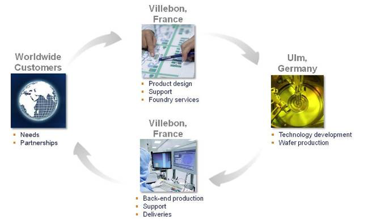
Figure A: UMS industrial flow
United Monolithic Semiconductors designs, manufactures and markets leading edge RF & millimeter-wave components and solutions for Defense, Security & Space, Telecom, Automotive and Industrial applications. Our in-house GaAs and GaN technologies offer state-of-the-art performance. Most of them are available in foundry mode.
UMS also offers a full range of catalogue products up to 100GHz based on GaAs, GaN and SiGe technologies, available in bare die and in SMD QFN leadless or in hermetic packages as illustrated in figure B for the different market.
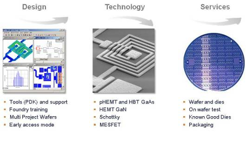
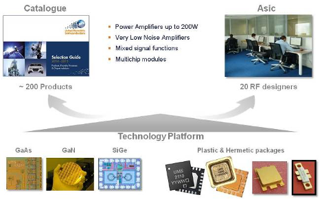
Figure B
UMS has developed and maintains several GaAs technologies for different microwave and mm-wave applications. Low-noise processes as well as high power processes are supported and available also for space projects. A strong collaboration with national and European space organisation has led to space evaluations for nearly all GaAs technologies offered.
Since several years UMS has developed AlGaN/GaN technologies (GH50, GH25 and GH15 with 0.5µm, 0.25µm and 0.15µm gate structures, respectively) well suited for highest power and best robustness.. Next year, UMS envisage to develop also a 0.1µm GaN based heterostructure for higher frequencies. The technology roadmap listing all UMS technologies and their development status is given in figure C. Please note that technologies with successfully performed space evaluation (to be listed in the EPPL = ESA European Preferred Parts List) are shown with a blue bar.
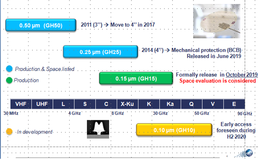
Figure C
UMS is dedicated to the achievement of total customer satisfaction. Villebon-sur-Yvette and Ulm plants are ISO9001, ISO14001 and ISO/TS 16949 certified.
Role
UMS is involved into the WP 6 (demonstrator) aiming to supervise the different demonstrators identified for WLP integration. As industrial, UMS has also a role of guidance about industrial aspects to consider during the development phase. It includes technology and economic aspects.
Key contribution
UMS is involved to support the manufacturing of demonstrators based on Wafer Level Packaging technology. The demonstrator referenced T6 is of interest. We will support also our partners to design and integrate test vehicles specially designed for reliability monitoring. For WLP, we are especially referring to environmental tests which are critical. The WLP process under evaluation is developed to address heterogeneous integration (GaN on SiC, Si and other materials). The role of the demonstrators and the different test vehicles would be to help for the development of the WLP building blocks.
In complement, UMS is involved into the evaluation of RF-MEMS process which is planned in a second demonstrator (T8). The object would be to evaluate the technological constraints facilitating the integration onto a passive process. A compatibility with WLP integration will be also considered too.
United Monolithic Semiconductors
10 Avenue du Quebec
91140 Villebon sur Yvette
France
Phone: +33 1 69 86 32 00
E-Mail: didier.floriot@ums-gaas.com
www.ums-gaas.com
![]()