Fraunhofer Institute for Microelectronic Circuits and Systems IMS
The Fraunhofer Institute for Microelectronic Circuits and Systems IMS is a research, service and contact partner for the development and pilot production of innovative microelectronic products and applications in an industrial environment.
Based in Duisburg, Fraunhofer IMS is one of more than 70 independent institutes of the Fraunhofer-Gesellschaft for the promotion of applied research, Europe's leading organization for industry-related research. In addition, our institute is part of the Fraunhofer Group for Microelectronics as well as the Research Fab Microelectronics Germany and is actively involved in numerous local, national and international networks of microelectronics and microsystems technology.
Fraunhofer IMS in Duisburg has more than 25 years of experience and proven expertise in microelectronic circuit design and fabrication. Our silicon solutions can be found in various application areas like satellites, aircrafts, medical implants, automotive, industrial, automation, and consumer electronics. Full supply chain services provide a seamless path from the first idea through development to production according to highest quality and reliability levels. This includes long term support considering our customers product lifetime requirements.
The focus of our research work is on offering solutions and developing marketable technologies and processes in the field of microelectronics that are used in many industries. As an independent institute, we have been working together with industrial and service companies as well as the public sector on projects for the direct benefit of the economy and society for more than 30 years. The scientists in our nine business segments contribute to the competitiveness of the region, Germany and Europe in accordance with the Fraunhofer-Gesellschaft's mission statement. We use science and research to promote innovation, strengthen technological performance, improve the acceptance of modern technology, and train and educate young scientists and engineers.
Fraunhofer IMS develops, fabricates and transfers CMOS and M(O)EMS technologies and devices for a broad range of applications within the business fields Mobility, Industry, Health and Space & Defense. The vision of Fraunhofer IMS is to extend the application areas of CMOS by post-processing on CMOS wafers to realize smart sensors e. g. pressure, image or bio sensors.
Development of new technologies and devices is one of the main activities at Fraunhofer IMS. We operate two cleanrooms (200 mm wafers). One is dedicated to CMOS technology and electronic devices and one for MEMS or NEMS processing with the option to use CMOS wafers (from IMS or external) as intelligent substrates (MST-Lab&Fab). Our services cover the whole range from providing single process steps to customer orientated technology and device development, qualification, and pilot fabrication.
In addition to the CMOS line Fraunhofer IMS operates its own microsystems technology line (MST Lab&Fab), which enables the post-processing of CMOS wafers and the integration of micromechanical, optical or other structures on the wafer to create new components. The microsystem technology (MST) and microelectronics become closely interlinked when it comes to the creation of compact” intelligent” sensors and actuators. MST should be seen as an extension of the CMOS technology: CMOS provides the electronics and MST delivers the sensor and actuator functions.
MST processes use semiconductor manufacturing equipment and profit from the diverse experience that the silicon semiconductor technology has built. If there are very small systems requested, small signals to be read out on short routes or there are arrays of sensors, the integration of the MST structures directly on the CMOS is recommended. The application possibilities of CMOS technology can be extended significantly without depending on expensive scaling to minute structures. That is why we at Fraunhofer IMS built our Microsystems Lab&Fab with the support of the state of NRW, the BMBF and the EU. In our facilities we use post-processing on CMOS to develop production processes and complete intelligent microsystems for our customers.
As a competent partner in the field of microsystem technology (development of process steps, process modules and complete microtechnological sensor systems) and their design Fraunhofer IMS offers various layer deposition, etching processes, 3D integration, lithography and so on for the Development and transfer of process modules for the production of” stand alone” MOEMS and functional micro structures like sieves, membranes etc.
For wafer testing Fraunhofer IMS is equipped with wafer probers and test systems for digital and analog tests. Besides electrical tests Fraunhofer IMS can also perform electro-optical tests for infrared imagers and optical sensor in the VIS/NIR spectrum.
Also Back-End processes such as wafer grinding and dicing, die and wire bonding or chip-to-wafer/ wafer-to-wafer bonding are part of Fraunhofer IMS portfolio, to provide the entire value chain during the product development.

Role
According to the project strategy, working together across multiple shareholders is required. Fraunhofer IMS as an R&D institute is a very experienced partner due to over 30 years cooperation with small and medium-sized enterprises (SME) or with large companies.
Within the joint ECSEL project iRel 4.0, the exploitation of Fraunhofer IMS will in general be focused on creating and expanding scientific expertise in the field of electronic reliability. Therefore, Fraunhofer IMS will work on aspects of reliability of optical sensors within the subproject "Reliability of optical sensors using the example of a LiDAR detector ". The work is also partly embedded within the Use Case T-4 “UC T-4 - Backside illuminated optical sensor”, which will be managed by Elmos Semiconductor SE and focuses on the reliability of LiDAR detectors, which are a core component for autonomous vehicles.
The UC T-4, which is mentioned before concentrates on the manufacturing and reliability prediction of a backside illuminated optical sensor system. The complete value chain will be considerate beginning with sensor and ROIC design and manufacturing, wafer bonding, assembly and test. For reliability prediction, all interfaces and materials must be considered as well as influences of contamination to performance and reliability (WP3). Because of different partners involved in the manufacturing and test process, a reliably data value chain must be enabled (WP2).
New test strategies have to be developed to enrich the electrical test by an optical functional test (WP5). Because of the addressed industrial and automotive market in safety critical applications, aspects of functional safety must be considered (WP4). The relevant application domain specifications and requirements will be derived in WP1.
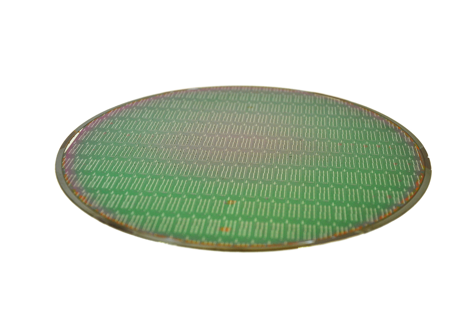
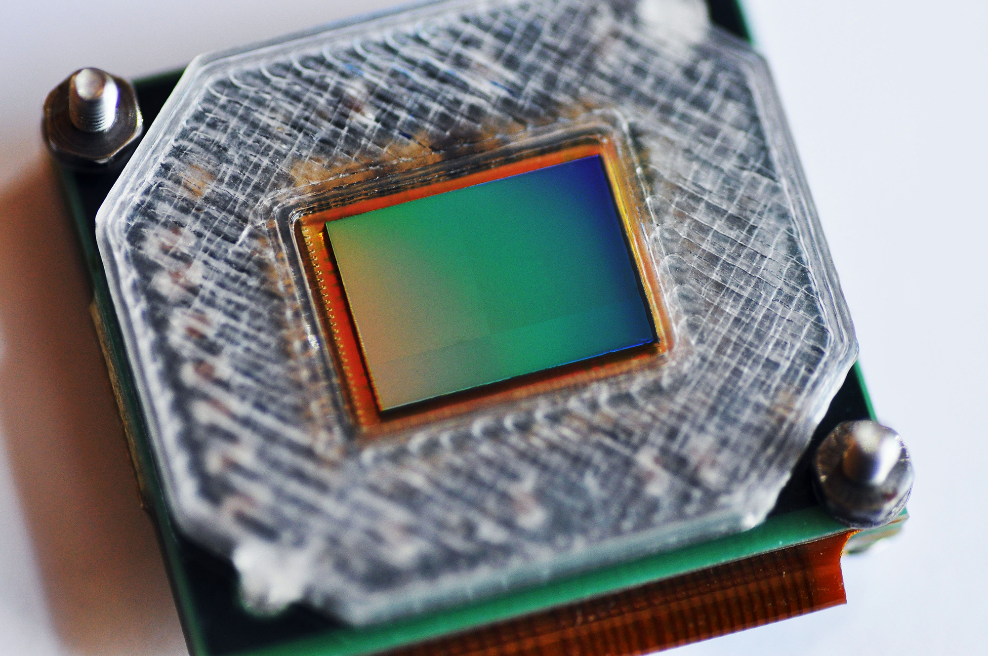
Fraunhofer IMS holds IP for several process technologies enabling the backside illumination (BSI) of optical or near infrared sensors. That is chip-to-wafer integration of readout wafer and sensor chip by means of solid-liquid-interdiffusion (SLID) bonding or, alternatively wafer-to-wafer bonding with direct oxide bonding. In both cases, process modules have been established for thinning the sensor wafer and thus enabling BSI. Currently only standard test methods, e.g. HTOL (high-temperature operating life), temperature cycling, vibration or shock according to the ACE-, JEDEC- or MIL-standard are used. Weak degradation e.g. of electro-optical performance is not considered by standard wafer-level tests. In particular high-speed electro-optical testing using wafer-level ATE is not established. A Backside illuminated optical sensor can be fabricated by bonding wafers produced by different manufacturers. Typically no deep measurement values are exchanged by these different manufacturers.
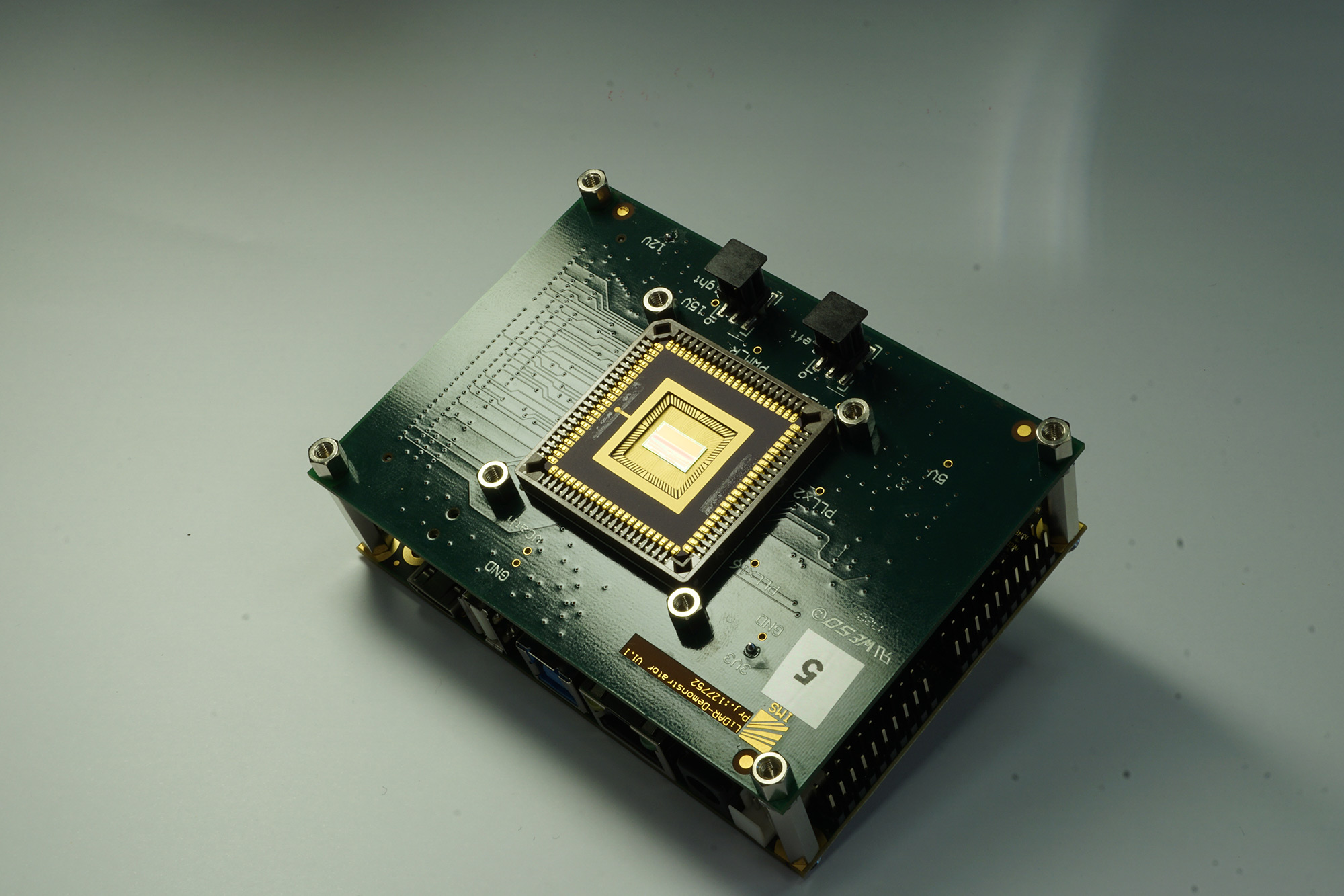
Fraunhofer will develop and fabricate a LiDAR sensor based on CMOS SPADs (single photon avalanche diodes) as a demonstrator with a globally leading lowest dark-count-rate. Additional outstanding parameters will be high uniformity, picosecond time resolution, and high sensitivity in blue and UV. Fraunhofer IMS will develop during this proposed project a wafer-level test system for LiDAR sensors. High speed electro-optical testing will be the main focus of this test system.
This use case will firstly demonstrate the use of optical sensors for safety critical applications including functional safety and a full data set of reliably data of all involved manufacturers. Fraunhofer will provide licensing of the developed technologies or methods to industrial partners of the consortium. Additionally the fabrication of pilot series or the wafer-level test of optical sensors can be performed by Fraunhofer IMS.
Key contribution
One main task will be the workouts of enhancements for the reliability of backside illumination (BSI) for optical or near infrared sensors. BSI of sensors requires precise thinning of the sensor wafer and this developed process will be offered to partners as a service or to potential customers by licensing. The optimization of the manufacturing processes of BSI have an important role within the contribution to WP3. The key process steps are the 3D-integration of optical sensors and CMOS circuitry, which contains void detection for wafer bonding with a surface acoustic microscope (SAM). This detection will be introduced in the integration process to enhance quality of the wafer bonding process. BSI of sensors requires precise thinning of the sensor wafer and demands smooth and clean surfaces for further post-processing. Both are difficult to achieve with common grinding and etching processes on typical silicon wafers. Smooth stopping on the low-impurity device layer with a reproducible remaining thickness will be addressed by developing a wet-etching process suitable for high-quality epitaxial substrates.
Another main task will be the development of an automated test equipment (ATE) on wafer-level for a LiDAR detector as an example for an integrated optical sensor within the contribution to WP5. According to the project strategy the contribution of Fraunhofer IMS will increase the coverage rate by advanced test concepts with new requirements.
Currently no standard ATE for different electro-optical parameters is available. Fraunhofer IMS will develop an innovative ATE for a LiDAR-detector as an example for an integrated optical sensor, which requires a dedicated test hardware and environment conditions. LiDAR-sensors are strongly requested for applications like automotive and industrial. High speed testing is one of the main focus for the development. This ATE will be used as a platform for the electrooptical characterization of different LiDAR detectors for German and European customers.
Furthermore, the Fraunhofer IMS will cooperate together with Elmos Semiconductor SE to work on the application use case "UC T-4: Backside illuminated optical sensor". The UC T-4 will be managed by the Elmos Semiconductor SE and concentrates on the production and reliability prediction of backside illuminated optical sensor systems. The entire manufacturing chain is considered. This starts with the design of the sensor and the corresponding readout circuit and continues with the manufacturing, wafer bonding, packaging and electro-optical testing.
Fraunhofer Institute for
Microelectronic Circuits and Systems IMS
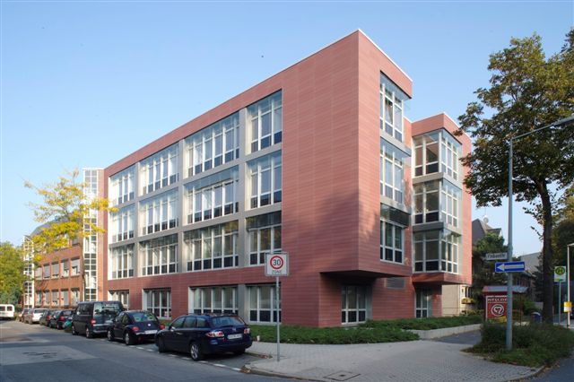
Finkenstraße 61
47057 Duisburg
Germany
Phone: +49 203 3783 227
E-Mail: info@ims.fraunhofer.de
www.ims.fraunhofer.de
![]()